Nitride semiconductor freestanding substrate production method
Able to product GaN at low cost by forming of nitride semiconductor crystal boules
Summary
Recently, III-nitride semiconductors (GaN and InGaN) have been
attracting attention as semiconductor materials for light-emitting devices
such as LED and lasers. This nitride semiconductor has a bandgap
energy with wide range wavelengths from infrared to ultraviolet light, and it
is a promising material for blue & green LED and semiconductor lasers
with UV to infrared region emission wavelengths. However, in the case of
nitride semiconductors, the equilibrium vapor pressure between the gas
and solid phases of nitrogen is much higher than the conventional III-V
materials, so it is not possible to fabricate GaN single crystal substrates at
low cost. Another option is to use freestanding GaN substrates, but the
current fabrication techniques are costly.
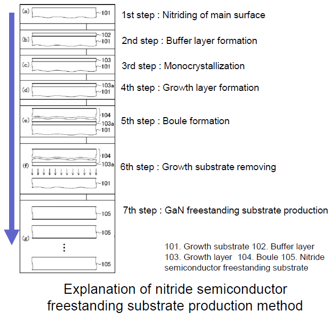
This invention is able to fabricate nitride semiconductor freestanding
substrates with low threading dislocation density at a low cost. This
invention comprises a total of seven steps, from the process of forming a
buffer layer having a nitride semiconductor on the growing substrate main
surface, to the process of fabricating a plurality of nitride semiconductor
freestanding substrates.

Effect
Fabrication of nitride semiconductor freestanding substrates at low cost by forming boules consisting of nitride semiconductor crystals
Application
・Light-emitting diodes, lasers, etc.
IP Data
IP No. : US patent 10,141,184, WO2016/132815
Inventor : MATSUOKA Takashi
keyword : Electronics, Hardware
