Real-time 3D optical imaging
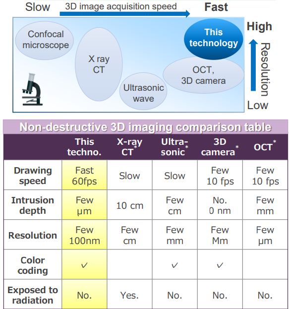
High speed, video-rate 3D imaging with a high spatial resolution like confocal microscopes
Overview
Various 3D imaging methods including X-ray CT, ultrasonography,and confocal laser scanning microscopy are employed in industrial applications, depending on its usage. However, X-ray CT requires the rotation of a light source or the irradiation area to acquire 3D images, which makes rapid imaging difficult. Ultrasonographyenables 3D measurement using 2D array elements but suffers from limited spatial resolution. In addition, confocal laser scanning microscopy requires the sequential acquisition of 2D images while moving the observation plane, which makes 3D observation at video rate impossible.
In recent years, 3D cameras and OCT are known as emerging 3D image acquisition techniques. However, the camera-based technique exploiting patterned- or line-illuminations provides limited spatial resolution, and it cannot visualize the internal information of samples. Besides, OCT is, in principle, applicable to reflected light signals only and impossible to measure fluorescence signals.A series of inventions solves the above issues and provides an imaging method with a simple implementation that enables the acquisition of precise 3D images in real-time.

Performance

Product Application
・Non-destructive inspection device for high-speed detection of extremely small defect
・Biological sample observation
・Observation of fast 3D microstructural deformation, etc
IP Data
IP No. :JP6537153, US10816474, DE112017002847.7,JP2019-117233, PCT/JP2021/031166
keyword : Measurement, Machine, Control
Optical information apparatus and microscope system
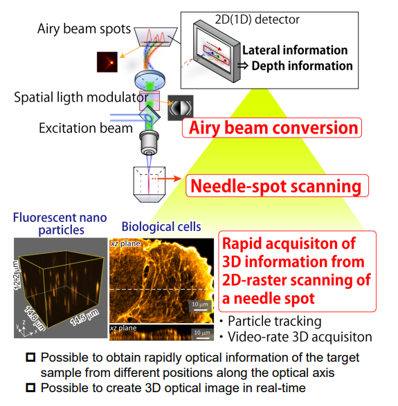
Rapid obtaining of optical information in the depth direction to create 3D optical image!
Overview
Laser scanning microscopy, used for observing a sample by scanning a laser focal spot and detecting reflecting, scattering, or fluorescence signals from a target can be increased acquisition speed of 2D images by high-speed raster scanning of a laser beam. But the rapid acquisition of 3D images is substantially
restricted due to the need of changing the moving observation plane.
Using the present invention can be possible the optical 3D imaging acquired at once without moving the optical system or target, because optical information along the optical axis obtained in different lateral position on the detector by separately concentrating the lights .

Product Application
・Rapid 3D image acquisition required domain
・Biological, organism-related and medical field such as bio-function analysis
・Industrial fields where the fine functional materials are developed such as metals and chemicals
Related Works
[1] Y. Kozawa and S. Sato, Sci Rep 9, 11687 (2019) https://doi.org/10.1038/s41598-019-48265-3
[2] Tohoku Univ. New Technology Presentation Meeting 2020, JST Seminar Video (Japanese Speaking)
IP Data
IP No. : JP6537153, US10816474, DE112017002847.7
Inventor : KOZAWA Yuichi
keyword : Measurement, Machine, Control
Holographic optical element and its manufacturing method
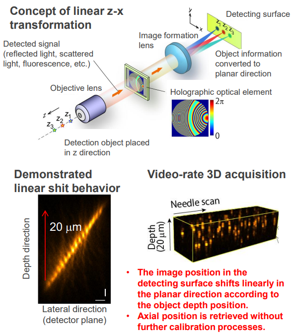
Conversion of depth information linearly into planar information!
Overview
In 3D imaging, it is important to effectively encode z information, which is the image formation displacement of the target object, into XY information, which is displacement from the optical axis of the image surface. On the other hand, in single-pixel imaging using only a single detector, it is important to encode in efficient manner the XY information of the target into the time information. However, the conventional encoding method has a limit on distance resolution, imaging distance range, z information decoding accuracy and encryption uniqueness.
This invention provides a new and improved hologram optical element, its manufacturing method and an optical device able to mutually convert Z & XY information with simple configuration. This invention is able to realize high accuracy and high spatial resolution for high-speed 3D imaging (patent US10816474) by converting the object depth direction information of the optical detection system into the planar direction information at the
detecting surface.

Product Application
・Optical field such as optical microscope
・Fast sensing for depth direction in 3D space
Related Works
[1] T. Nakamura et al., Opt. Lett. 43, 5949 (2018).
[2] Y. Kozawa et al., Biomed. Opt. Express 13, 1702 (2022)
[3] Press release (Tohoku Univ.)
IP Data
IP No. : JP7021772
Inventor : NAKAMURA T., IGARASHI S., KOZAWA Y
keyword : Measurement, Machine, Control
Spot light generator, optical information detection device and microscope
Fast 3D imaging without the need of multi photon excitation
Overview
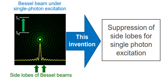
High-speed 3D imaging achieved by scanning a non-diffractive, needle-like spot provides high XYZ resolution. The light-needle-spot is produced by a Bessel beam with extended side lobes, which is known to cause artifacts in the acquired images.
To reduce the influence by the side lobes, a multiphoton excitation process including two-photon excitation is generally used for fluorescence imaging. Accordingly, a microscope system requires a near-infrared, ultrashort pulsed laser source, which significantly rises in the initial cost. In addition, the need for the multiphoton excitation process limits observation targets to fluorescence imaging only.
This invention provides a method to generate a needle spot using a simple configuration that can suppress side lobes, without two photon excitation, using a visible light source available on the market. This invention can be applied to high-speed 3D imaging for surface inspection and profiling by detecting reflected or scattered light signals in addition to the fluorescence signal

Features

Product Application
・Non-destructive inspection to detect & remove refined 3D defects, etc.
・Bioimaging
・Surface profiling
Related Works
[1] Japan Society of Applied Physics 82nd autumn meeting 2021 presentation document
[2] Patent US10816474 → T15-198
IP Data
IP No. : PCT/JP2021/031166
Inventor : KOZAWA Yuichi
keyword : Measurement, Machine, Control
