Optical nanoimprinting method that enables a uniform residual layer without burr generation at mold edge
Precise manufacture of complicated structure with sparse/dense micro/nano-patterns!
Overview
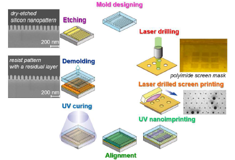
Ultraviolet nanoimprint lithography (UV-NIL) have attracted attention as an industrially acceptable nanofabrication technology from views of cost and throughput; However, the use of spincoated films of photo-curable resin on substrates causes the problems of burr generation arising from mold edges and unleveled residual layers arising from site-selective differences in pattern densities of mold surfaces. The problems make subsequent lithography processes impossible. This optical nanoimprinting method consists of micro-scale laser-drilled screen printing and nano-scale molding. High-viscosity photo-curable resins with 1-300 Pa・s can be placed by screen printing using a polyimide sheet having through poles which are fabricated by laser drilling using a picosecond pulsed laser. The minimum volume of a printed droplet is 5 fL (10-15L). The resist patterns and resultant silicon patterns with 45-nm-linewidths are fabricated.

Nanofabrication by laser-drilled screen printing

Product Application
Optics: microlens array, polarizer, antireflection surface, metalens
Electronics: metal/semiconductor/insulator patterning, built-up devices
Bio applications: culture sheet, nano/micro fluidic device
Related Works
1. Jpn. J. Appl. Phys., 2016, 55, 06GM01
2. J. Vac. Sci. Technol. B, 2016, 34, 06K404
3. J. Vac. Sci. Technol. B, 2017, 35, 06G301
4. Bull. Chem. Soc. Jpn., 2018, 91, 178
IP Data
IP No. : JP6005698, US10613433
Inventor : NAGASE Kazuro, IKEDO Hiroaki, UEHARA Takuya,NAKAGAWA Masaru
keyword :Electronics, Hardware
