Method of manufacturing semiconductor package and its package
It provide a manufacturing method that can suppress die shift
Overview
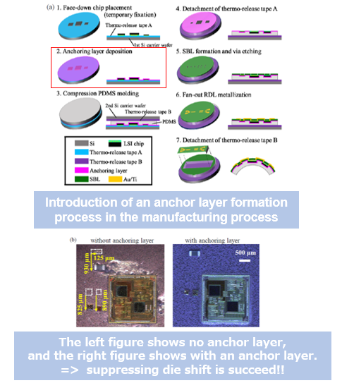
The Fan-out Wafer Level Package (FOWLP) method, which is the mainstream method for semiconductor packages, especially for mobile applications, has a problem of "die shift" in which mounted components shift by flow of sealing resin and wiring defects occurred. Further, even in a device such as a flexible display, there is a problem that a mounted component on the device is shifted when the device is bent.
In order to solve the above problems, the invention is a method of manufacturing a semiconductor package without die shift by incorporating a special anchor layer under a mounting component and adopting a special manufacturing process, and the semiconductor package.
The invention is expected to produce a highly integrated semiconductor package without a die shift, and to be applied to a flexible display and a wearable device.
Features・Outstandings

Product Application
・μ-LED Flexible Display
・Semiconductor package for flexible wearable device
Related Works
[1] T. Fukushima et al., IEEE Transactions on Components,Packaging and Manufacturing Technology, vol. 10, no. 8, pp.1419-1422, Aug. 2020
IP Data
IP No. : WO/2022/025214
Inventor : FUKUSHIMA Takafumi, TANAKA Toru, KINO Hisashi, SUSUMAGO Yuki
keyword : semiconductor packages, die shift, flexible
